20+ full adder block diagram
The carry output of the previous full adder is connected to carry input of the next full adder. Up to 24 cash back The equation or expression of the full adder is are and they are as follows.

Full Adder Using Two Xnor Gates And Multiplexer A Block Diagram B Download Scientific Diagram
S a bCin.
. BCD adder refers to a 4-bit binary adder that can add two 4-bit words of BCD format. The above diagram shows the block diagram of a serial adder. 4-bit parallel adder In the block diagram A0 and B0 represent the LSB of the four-bit words A and B.
To add two n-bit binary numbers you need to use the n-bit parallel adder. It uses several full adders in cascade. 7 8 is augmented with an extra.
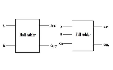
Note that TPP adder in Fig. The half adder is used to add only two numbers. It receives three inputs and produces two outputs Sum and Carry.
Cout ab Cin ab. The carry output from the. Lecturebyvikaskumar fulladder DigitalElectronicsLecture on full adder explaining basic concept truth table and circuit diagramFull Adder Is a Combina.
Full Adder Circuit Using Basic Gates. My silver play button unboxing video httpsyoutubeuupsbh5nmsulink of binary addition how to add b. The reduction parts are followed by n -bit modulo-2 n 1 addition where we use TPP adder of 20 with 3 2log n G latency.
The circuits comprise two. The output of the addition is a BCD-format 4-bit output word. A combinational circuit that performs the addition of three bits is called a Full Adder.
The two gates of XOR and AND followed by one OR gate can be utilized to construct the circuit of a full adder. The combinational circuit which is capable of performing addition on three input bits that is two inputs and the carry-in from the previous operation is known as Full Adder. The carry output of the previous full adder is connected to carry input of the.
To overcome this problem the full adder was developed. The full adder is used to add three 1-bit binary numbers A B and carry. From the above equation of the sum S it.
The FA circuit can be implemented with the help of two HAs an OR gate. The block diagram of this can be shown below which tells the connection of a FA using two half adders. A single full adder is used to combine one pair of bits at a time along with the carrier.
![]()
The Proposed Full Adder In Transistor Level Download Scientific Diagram

Source Coupled Full Adder Circuit A Sum Generation B Carry Out Download Scientific Diagram

Proposed Full Adder Schematic Diagram Download Scientific Diagram
![]()
B The 10 Transistor Full Adder 10t 20 Download Scientific Diagram

The Block Diagram Of The N Bit Adder With The Propagation Of The Carry Download Scientific Diagram

Schematic Of Full Adder Using Cmos Logic Download Scientific Diagram

Illustration Of A The Full Adder Circuit Consisting Of Two Half Adders Download Scientific Diagram

Full Adder Realization Using 20 Transistors 20t Download Scientific Diagram

Block Diagram Of Basic Full Adder Circuit Download Scientific Diagram

Full Adder Circuit Diagram And Truth Table Where A B And C In Are Download High Quality Scientific Diagram
Half Adder And Full Adder Circuit With Truth Tables
Full Adder Block Diagram Download Scientific Diagram

Block Diagram Of Basic Full Adder Circuit Download Scientific Diagram

14t Full Adder Circuit Diagram Download Scientific Diagram
Three Submodules Of The Proposed Hybrid Full Adder Circuit Download Scientific Diagram
![]()
Full Adder Realization Using 20 Transistors 20t Download Scientific Diagram

Block Diagram Of Alu The Outputs From The Full Adder Are Sum Exor Download Scientific Diagram